
Close Menu
  • News
  • Industry
  • Solar Panels
  • Commercial
  • Residential
  • Finance
  • Technology
  • Carbon Credit
  • More
    • Policy
    • Energy Storage
    • Utility
    • Cummunity
What's Hot

Distributed solar capacity in Argentina grew by 34.5% in the first half of the year

July 23, 2026

The UK government has urged to ensure that plug-in solar is properly regulated

July 22, 2026

Cornwall Insight cuts price ceiling forecast after Burnham’s VAT cut

July 22, 2026
Facebook X (Twitter) Instagram
Solar Energy News
Thursday, July 23
  • News
  • Industry
  • Solar Panels
  • Commercial
  • Residential
  • Finance
  • Technology
  • Carbon Credit
  • More
    • Policy
    • Energy Storage
    • Utility
    • Cummunity
Solar Energy News
Home - Technology - Assessment of fractures in the processing of monocrystalline G12 wafers – SPE
Technology

Assessment of fractures in the processing of monocrystalline G12 wafers – SPE

solarenergyBy solarenergyOctober 14, 2024No Comments3 Mins Read
Facebook Twitter Pinterest LinkedIn Tumblr Email
Share
Facebook Twitter LinkedIn Pinterest Email

Scientists in China have investigated the fracture strength of commercial G12 monocrystalline wafers through the 4-point bend test and found that the thickness of the wafer, the position of the silicon wafer in the silicon brick and the bend test direction are key parameters for developing future strategies. aimed at reducing fractures.

October 14, 2024 Emiliano Bellini

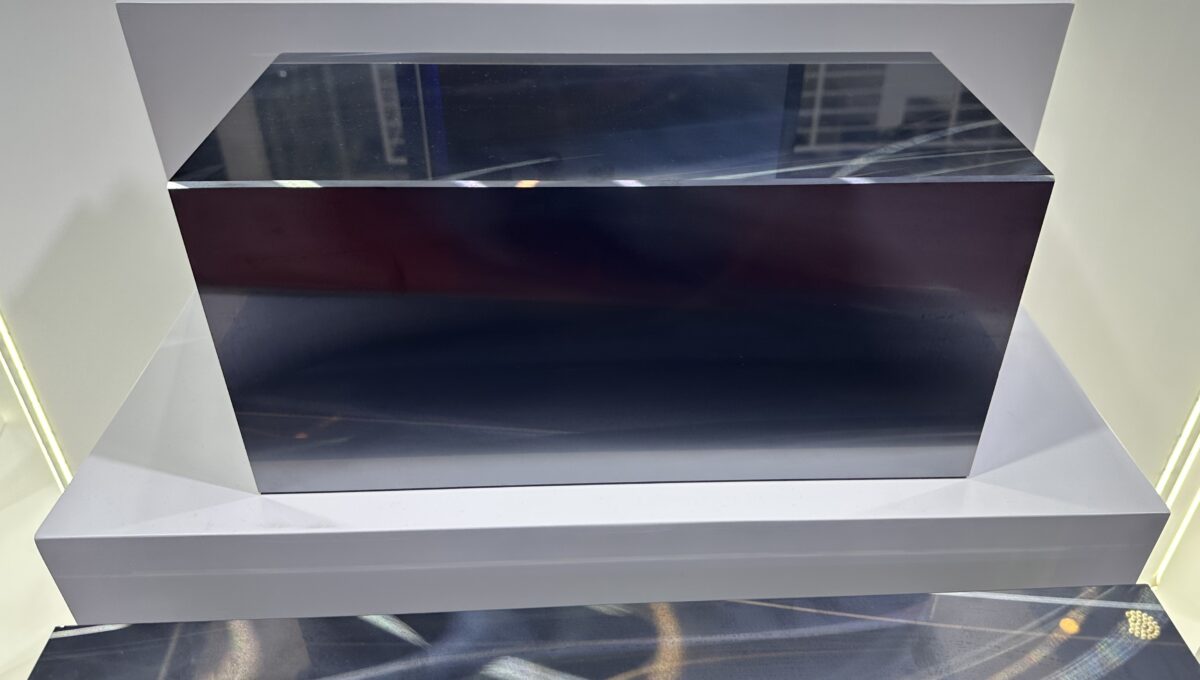
Researchers from Shandong University in China have investigated the fracture strength of commercial 210mm x 210mm monocrystalline silicon G12 wafers used for solar cell production and found that several strategies can be applied to produce large and ultra-thin silicon wafers and at the same time to reduce the breakage. probability during the sawing process and post-processing.

“We investigated the effect of wafer thickness on the fracture strength and the effect of the position of the silicon wafer in the silicon brick on the fracture strength of the silicon wafer,” says the lead author of the study. Yufei Gao, told pv magazine. “Four-point bending (PB) tests were performed on three thicknesses of G12 mono-Si wafers, and the load-displacement curves during the testing process were recorded.”

This type of testing is used to assess the flexural strength of a material and its tendency to crack under the flexural load. The material is usually placed on two support pins and loaded centrally onto two pressure lines with a test piston.

For their analysis, the researchers used the finite element method (FEM), a numerical technique used to perform finite element analysis (FEA) of any given physical phenomenon, and the Weibull function, which is most commonly used in analyzing of silicon wafers. breakage.

See also  Copper Doping stimulates the stability of the manganese cathode in sodium batteries-PV Magazine International

“The basic assumption of the Weibull function is the weakest link assumption: the survivability of a sample is the product of the survivability of each volume element in the sample,” the scientists explained. “Therefore, the fracture strength of silicon wafers is determined by the weakest defect.”

They analyzed three different wafer thicknesses of 130 urn140 urnAnd 150 μm and took into account the position of the silicon wafer in the silicon brick and the bending test direction.

The analysis showed that the surface roughness of the wafers decreases as the usage time of the sawing wire increases. It also showed that the curvature of the saw marks on the wafer surface increases with the increase of the saw wire usage time.

Furthermore, the team found that the distribution of the fracture probability density curve is more concentrated in the front wafers, while it is more spread out in the back wafers. It was also found that the fracture characteristics of the center wafers and the rear wafers are similar.

They also found that the characteristic breaking strength of bending in the perpendicular direction to the saw marks is two or three times that of bending in the parallel directions to the saw marks.

“The relationship between the saw wire usage time, surface roughness and saw mark characteristics with the fracture strength of silicon wafers has been revealed, which provides the improvement direction for improving the strength of large ultra-thin silicon wafers and reducing the fracture probability in the production process ,” said the academics.

See also  GCL breaks ground for a 2.4 GW pumped storage facility in China – SPE

This content is copyrighted and may not be reused. If you would like to collaborate with us and reuse some of our content, please contact: editors@pv-magazine.com.

Popular content

Source link

Assessment fractures G12 monocrystalline processing SPE wafers
Share. Facebook Twitter Pinterest LinkedIn Tumblr Email
solarenergy
  • Website

Related Posts

EVelution Energy is pioneering a solar-powered cobalt processing facility

July 1, 2026

Pexapark registers 17 European PPAs for 966 MW in April – SPE

May 27, 2026

Saudi Arabia gets first BESS production facility – SPE

May 27, 2026
Leave A Reply Cancel Reply

Don't Miss
News

Solarbank and Viridi partner on 3-MW Community Solar + Storage project at closed landfill

By solarenergyFebruary 20, 20250

Solarbank has announced that it cooperates with Viridi, producer of Fail-Safe Battery energy storage systems…

SolarAPP+ streamlines the solar permitting process

May 20, 2024

York Minster selects installer for cathedral solar installation

July 24, 2024

First Citizens Bank finances BESS

May 16, 2024
Stay In Touch
  • Facebook
  • Twitter
  • Pinterest
  • Instagram
  • YouTube
  • Vimeo
Our Picks

Distributed solar capacity in Argentina grew by 34.5% in the first half of the year

July 23, 2026

The UK government has urged to ensure that plug-in solar is properly regulated

July 22, 2026

Cornwall Insight cuts price ceiling forecast after Burnham’s VAT cut

July 22, 2026

SmartestEnergy, Greentech ink CfD PPA for the Kent solar project

July 22, 2026
Our Picks

Distributed solar capacity in Argentina grew by 34.5% in the first half of the year

July 23, 2026

The UK government has urged to ensure that plug-in solar is properly regulated

July 22, 2026

Cornwall Insight cuts price ceiling forecast after Burnham’s VAT cut

July 22, 2026
About
About

Stay updated with the latest in solar energy. Discover innovations, trends, policies, and market insights driving the future of sustainable power worldwide.

Subscribe to Updates

Get the latest creative news and updates about Solar industry directly in your inbox!

Facebook X (Twitter) Instagram Pinterest
  • Contact
  • Privacy Policy
  • Terms & Conditions
© 2026 Tsolarenergynews.co - All rights reserved.

Type above and press Enter to search. Press Esc to cancel.