Researchers in India have shown that ion beam implantation enables precise boron doping in silicon solar cells, reducing defects and improving charge transport. The proposed approach could support more efficient and reproducible p-n junctions, which could provide a path to higher performance silicon photovoltaics.
Researchers from Panjab University in India have demonstrated a new method for doping silicon solar cells using ion beam technology, achieving improved electronic properties and reducing losses due to defects.
“Defects in TOPCon and PERC solar cells often arise from conventional manufacturing processes such as thermal diffusion, radio frequency (RF) sputtering and plasma-based techniques, where limited control over the doping concentration leads to non-uniform p-n junction formation,” said corresponding author Monika Verma. pv magazine. “These proven methods can introduce lattice distortion, uneven doping profiles and defect complexes, which reduce carrier lifetime and limit charge transport, ultimately reducing efficiency.”
Ion beam implantation offers a way to alleviate these problems by allowing precise control over doping depth and concentration, reducing impurity-related defects, and improving the transport properties of carriers. It also supports advanced device architectures through uniform and repeatable junction formation.
The technique involves focusing high-energy ions into a material to change its composition and structure at the atomic level. It is widely used in semiconductor manufacturing to implant dopants, allowing controlled formation of p-n junctions with minimal defects and improved electronic performance.
“Ion beam technology has long been used in the integrated circuit industry and is now re-emerging as a promising tool for photovoltaic applications,” says co-author Sanjeev Gautam. “It provides precise control over dopant concentration, uniform ion distribution and adjustable junction depth based on ion energy and fluence, improving reproducibility.”
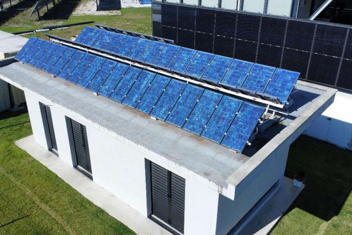
Image: Panjab University
The researchers fabricated an ap-n junction by implanting boron ions into n-type silicon wafers at an energy of 35 keV. Compared to conventional thermal or plasma-based methods, the ion beam approach allows highly controlled placement of dopants while minimizing structural damage.
They confirmed the uptake of boron using X-ray photoelectron spectroscopy (XPS), observing a measurable shift in silicon’s binding energy. According to the study, XPS showed higher sensitivity than traditional techniques such as X-ray diffraction (XRD) and Rutherford backscattering spectrometry (RBS) for detecting implanted dopants. Additional analysis using Near-Edge X-ray Absorption Fine Structure (NEXAFS) spectroscopy revealed changes in the local electronic structure consistent with boron integration into the silicon lattice.
“Boron implantation in n-type Si(100) creates a p-type layer, which forms the p-n junction,” says Verma. “Measuring dopant concentration is challenging because many conventional techniques fail to detect low levels.
Electrical tests revealed diode-like current-voltage characteristics consistent with the Shockley model, confirming the formation of a functional p-n junction. The devices showed a low leakage current of approximately 0.63 mA, indicating reduced recombination losses and improved charge transport.
The researchers attributed these improvements to minimized lattice defects, a major limitation in standard production of silicon solar cells. Such defects typically act as recombination centers, shortening carrier lifetime and overall efficiency.
“With this work, we demonstrate how ion implantation can be used to fabricate p-n junctions under controlled conditions,” says Gautam. “Dopants are introduced into Si(100) with defined energy and fluence, forming a thin layer on the nanometer scale. The goal is to minimize crystal damage, much of which can be repaired after implantation, providing a path to the next generation of high-efficiency silicon solar cells.”
The new approach was presented in “Accurate detection of dopants and transport properties of boron ion-implanted silicon solar cells”, published in RSC progress.
This content is copyrighted and may not be reused. If you would like to collaborate with us and reuse some of our content, please contact: editors@pv-magazine.com.
Popular content